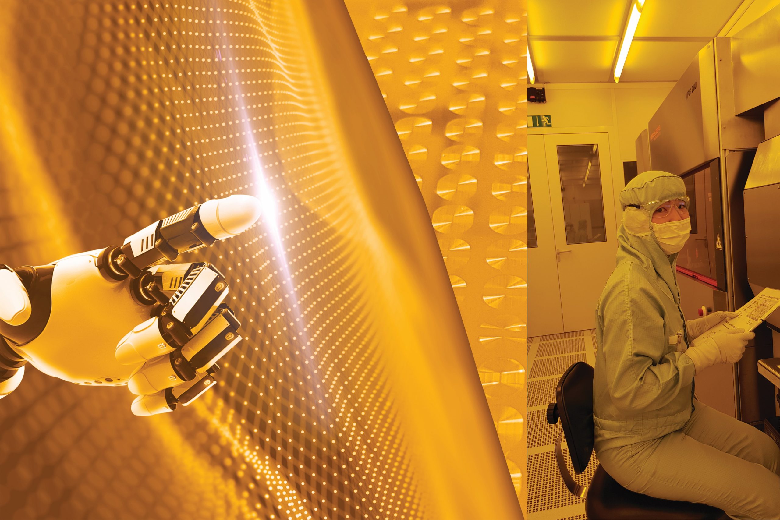
CUSTOMIZED ULTRA THIN FLEXIBLE MICROCIRCUITS
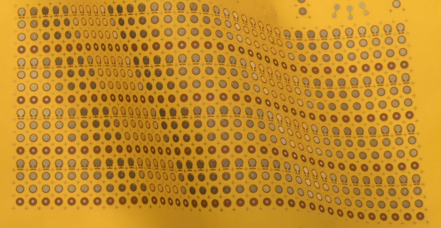
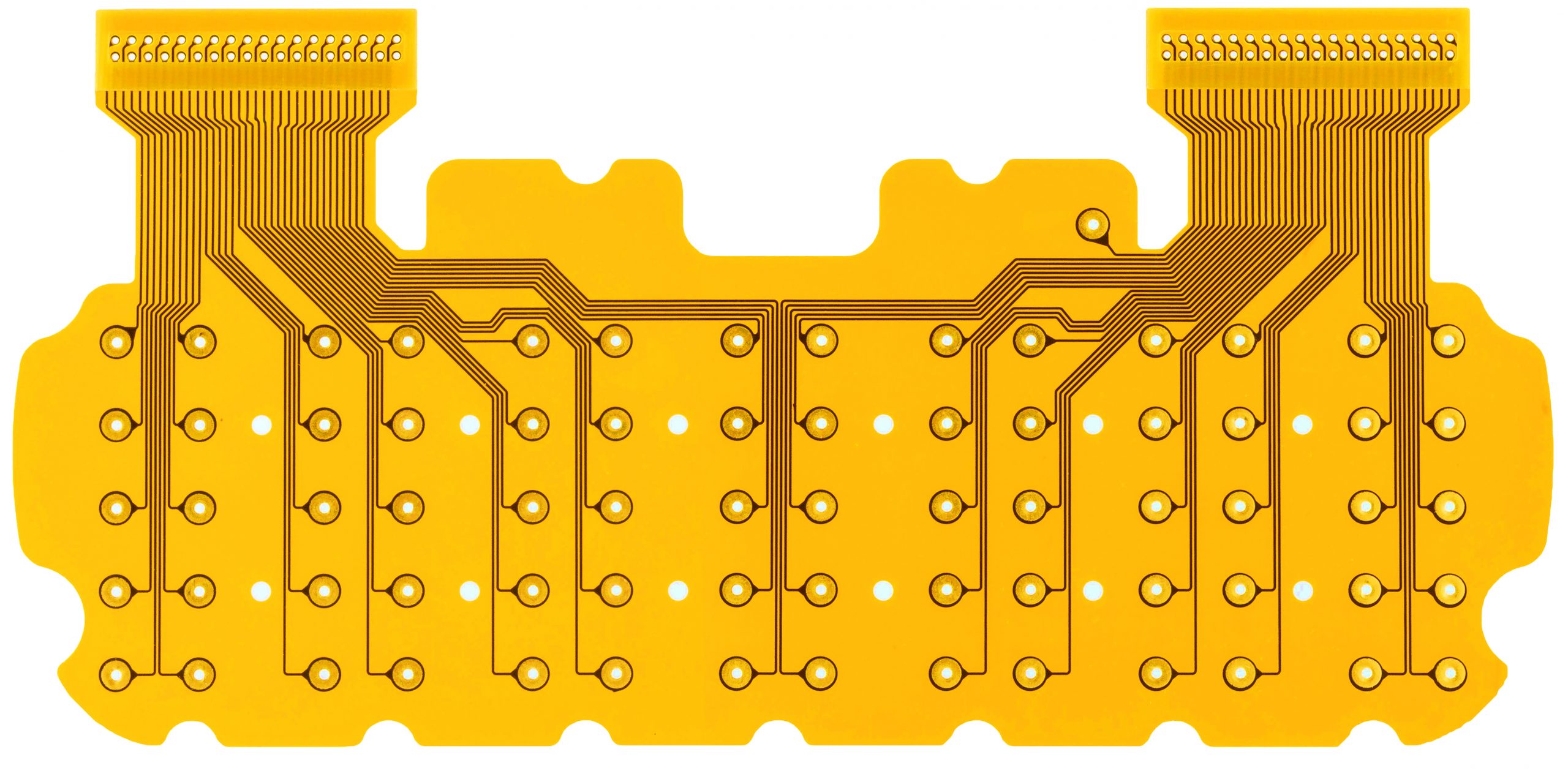
Our ultra-thin flexible microcircuit technology provides unlimited designs and production possibilities, with high miniaturizing complex and ultra-compact which highly in demand in different high technological applications seeking for miniaturization.
We are active in the field of flexible thin film technology on Polyimide and Thin & Thick film on Ceramics and Glass based materials for all kind customized designs to development and manufacturing ultra-thin flexible microcircuits.
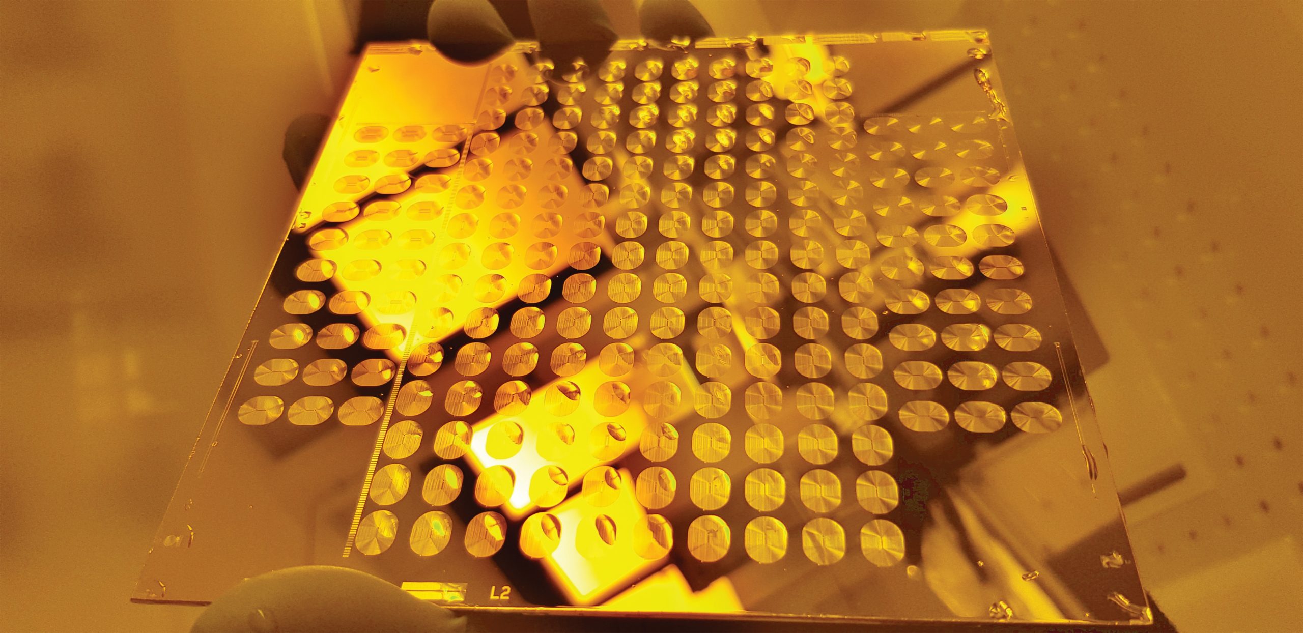
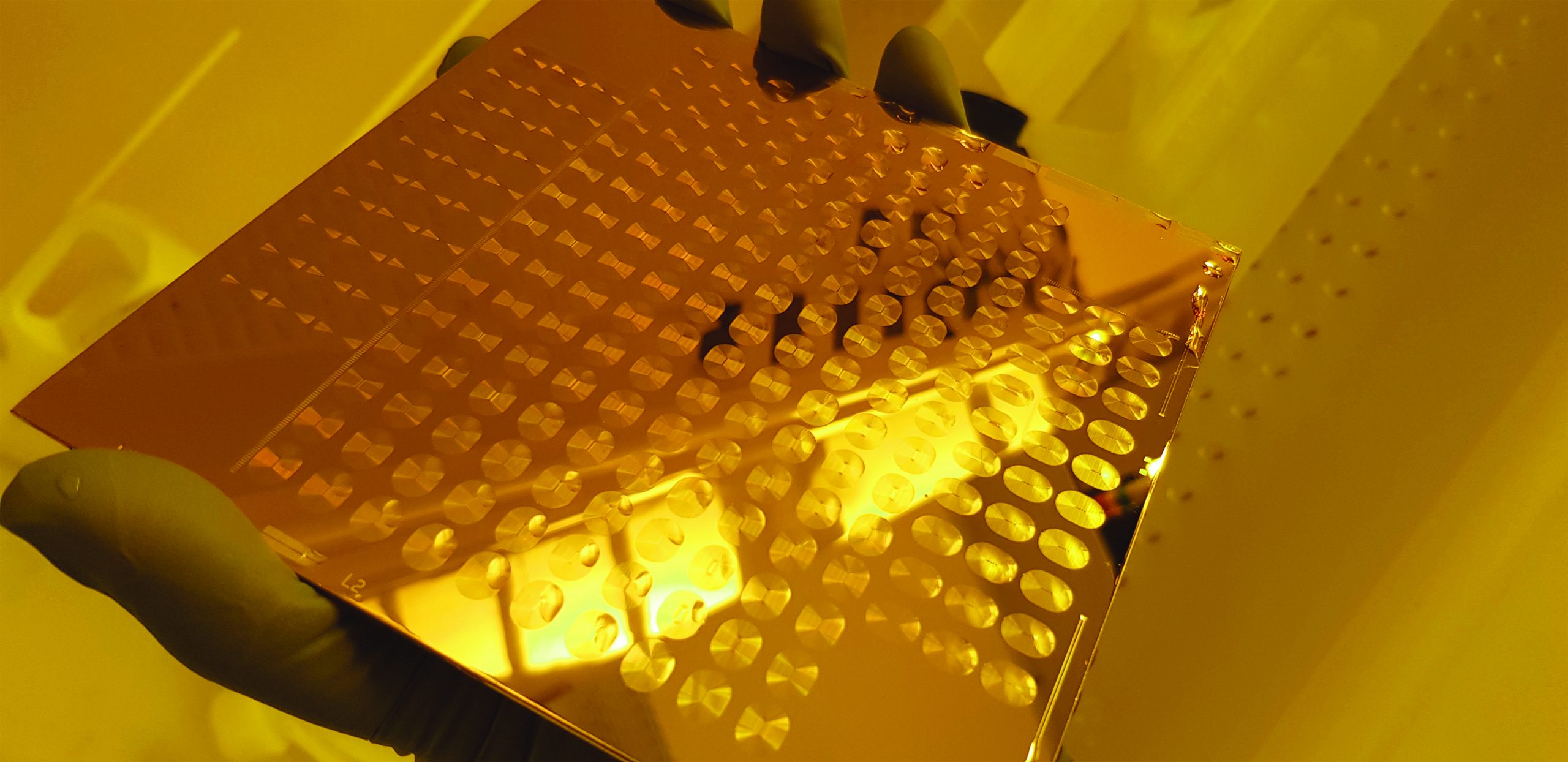
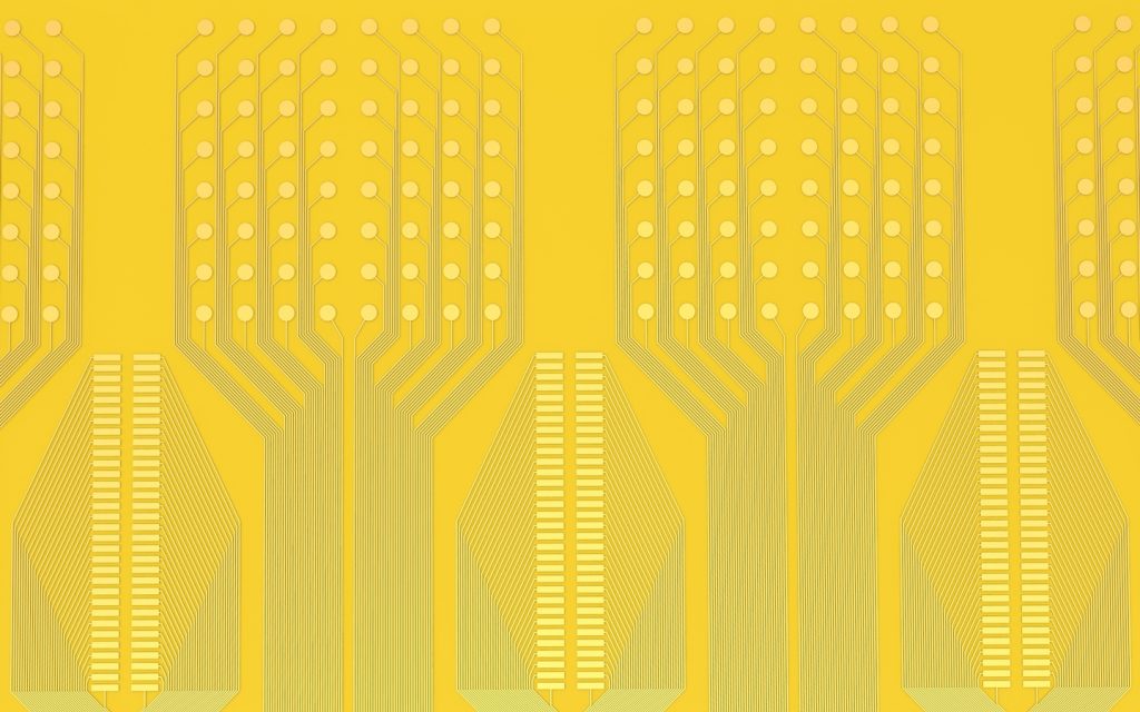
Our technology is a highly flexible microcircuits technology with ultra finely patternable interconnects with a pitch of 10 microns. In addition to standard products, this interconnects reduced by a factor of 10, resulting in corresponding savings resulting surface to 16 times more smaller comparing to other FPC technology.
We design and produce customized circuits with a wide choice of materials up to 5 layers including conductive layers in submicron levels (40nm to 12µm thickness) with high densities interconnection and a total thickness less than 60µm with high innovative thin film circuit technology.
Strong demand in medical ultra long flexible microcircuits and interconnection with highly miniaturized thinner, multilayer and lighter devices where the current printed technology is struggling and limited, our flexible microcircuits technology offers great advantages like imaging catheter diagnostics devices, endoscopes and ablation catheters with long multilayer flexible cables integrated with active components solutions.
Customized thin film metallization consists of sputtering metal layers with patterns made to customer specifications.
SWISSFLEX MICROCIRCUITS AG is able to deposit a wide variety of films on many different substrate materials (Silicon, Glass, Alumina, Insulated Metal Substrates like Aluminium and Copper).
We are using 3 targets in-line sputtering systems in order to provide willing film quality and access to custom adhesion, barrier and conductive layers.
The target materials available at SWISSFLEX MICROCIRCUITS AG include Chromium, Titanium, Copper, Gold, Platinum, Aluminum, Tungsten, Tantalum, Silver, and Chromium Nickel alloys.
Depending on the material selected needs, thin film sputtered layers can range from 25 nm for adhesion layers to 9um for conduction layers. Patterning is done to match customer specifications using wet chemical etch processes, dry etch processes, lift-off processes, liquid or dry photoresist processes, fine thin film line patterns and in circuit test measurement.
SPUTTERING
| Metallization for flex circuits | Material | Thickness Range SPUTTERED | Typical Thickness |
| Conductive Layers | Au,
Cu, Ni, Al |
0.1 µm to 1.5 µm
0.1 µm to 1.0 µm 0.1 µm to 1.0 µm 0.1 µm to 1.0 µm |
0.10 µm
0.60 µm 0.02 µm 0.30 µm |
| Diffusion Barrier Layers: | Ni,
Pt, Pd, TiW, Mo, NiCu |
0.05 µm – 0.2 µm
0.05 µm – 0.2 µm 0.07 µm – 0.15µm 0.03 µm – 0.06 µm 0.05 µm – 0.2 µm 0.05 µm – 0.2 µm |
0.02 µm
0.10 µm 0.10 µm 0.05 µm 0.60 µm 0.60 µm |
| Adhesion Layers | Cr,
NiCr, Ti, TiW |
0.02 µm – 0.01 µm
0.02 µm – 0.25 µm 0.02 µm – 0.01 µm 0.02µm – 0.06µm |
0.03 µm
0.05 µm 0.06 µm 0.05 µm |
| Resistive Layers | Ta2N,
NiCr |
0.02 µm – 0.15 µm
0.02 µm – 0.25 µm |
0.05 µm
0.05 µm |
| Substrates | Glass,
Si, AlN, Alumina SOI |
4 inch x 4 inch
6 inch x 6 inch 8 inch x 8 inch
|
ELECTROPLATING
| Metallization for flex circuits | Material | Thickness Range ELECTROPLATED | Typical Thickness |
| Conductive Layer | Cu | 1.0-7.0 | 4.0 |
| Diffusion Barrier Layer | Ni | 0.5-7.0 | 1.5 |
| Diffusion Barrier Layer | Pd | 0.5-1.5 | 0.5 |
| Solder Layer | Au | 0.1-2.0 | 1.2 |
| Solder Layer | Sn | 0.5-8.0 | 1.5 |